New development
We develop geometry, circuitry and integration based on your frequency bands, installation conditions and measurable target values.
CONTRACT DEVELOPMENT
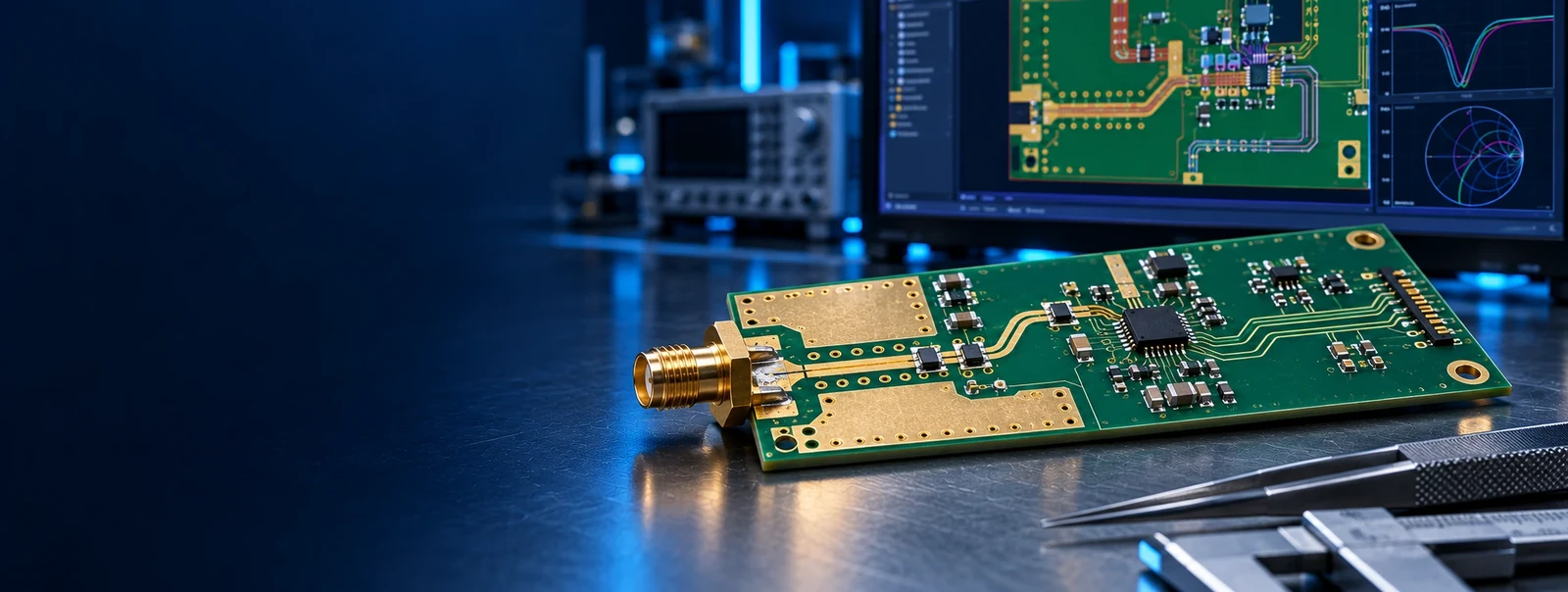
We check and optimize circuit boards from the antenna connection to the RF chip. This includes component placement, line geometry, reference planes, ground and return current routing as well as all transitions between components, layers, cables and connectors. We provide support before the first prototype, in case of inadequate wireless performance and when redesigning an existing product.
01 / TECHNOLOGY & DEVELOPMENT
A nominal 50 Ω trace is not sufficient if reference planes are interrupted or connections and layer changes create strong discontinuities. We check the real circuit board structure including material, copper geometry, ground distances and manufacturing constraints.
02 / TECHNOLOGY & DEVELOPMENT
We trace the complete signal path through antenna, matching, filter, LNA and radio chip. Pads, component terminals, connector launches, and coax connectors are considered electrical structures. Sensitive reception stages, clock sources, switching regulators and digital lines are arranged in context.
03 / TECHNOLOGY & DEVELOPMENT
We examine selected critical transitions using electromagnetic simulation and, if a prototype is available, compare them with measurements. This makes it possible to distinguish whether the cause lies in the antenna, a mismatch, line losses, coupling or the supply. Not every layout point requires the same model: the testing effort depends on the risk and target value.
04 / TECHNOLOGY & DEVELOPMENT
You receive specific locations for changes, prioritized by technical effect. We can coordinate the proposals with your layout team or undertake an agreed redesign. After building the modified prototypes, we check whether the measures improve the intended properties.
THREE WAYS TO THE RIGHT SOLUTION
We develop geometry, circuitry and integration based on your frequency bands, installation conditions and measurable target values.
We analyze existing samples and documents, determine the cause of losses or inadequate performance and implement targeted changes.
We check an existing Sevskiy solution and adjust frequency tuning, connections or installation. We can handle mass production upon request.
OUR APPROACH
We clarify the frequency plan, installation space, mechanical environment, supply, connections and test criteria. Existing CAD, circuit and measurement data are incorporated.
We compare suitable concepts, design the circuit or geometry, and simulate critical electromagnetic structures and transitions.
We build prototypes, measure under defined conditions and fine-tune the design based on the comparison between the model and the real structure.
We document the agreed design and test plan. Production support and management of mass production are agreed as required.
YOUR RESULT
You receive an RF layout review with prioritized findings or a revised layout with documented boundary conditions and agreed comparison with measurement results. New development, optimization of existing PCBs and integration or customization of existing RF components are possible.
FREQUENTLY ASKED QUESTIONS
Before the release of the first prototype and in the event of insufficient range, weak GNSS reception, unexpected attenuation, harmonics or mutual interference between several radio services. An early review can reveal critical areas before PCB production.
No. We narrow down the affected signal path and check whether targeted changes to placement, matching, reference planes or transitions are sufficient. A complete redesign is only agreed as a separate scope.
Circuit diagram, PCB layout, layer stack and material data, parts list and, if possible, mechanical drawings, samples and existing measurement results. We coordinate the exchange of confidential data directly.
SERVICES IN DETAIL
YOUR RF TASK
We will clarify with you whether a new development, optimization or product customization makes sense.