SERVICES

Antenna development and RF system design

New development, optimization or product customization: We take on the technical tasks along your entire RF signal path.

COLLABORATION

Three starting points. A continuous development process.

01

New development

Frequency plan, installation space, interfaces and target values form the basis for concept, simulation, circuit, layout and prototype.

02

Optimize existing designs

We measure the current state, locate the limiting point and specifically change the antenna, matching, layout or integration.

03

Customize an existing product

We check our product range and adapt frequencies, connections, cables or mechanics to your device.

SYSTEM CONSIDERATION

From the antenna to the radio chip.

  1. 01AntennaRadiation and reception
  2. 02MatchingImpedance and matching
  3. 03Filter/LNASelectivity and noise
  4. 04Cable / connectorLosses and connection
  5. 05PCB / TransitionsCable routing and coupling
  6. 06RF chipRadio module and interface

The order and combination of the components depends on the send and receive path. We consider impedance, attenuation, noise and coupling at each interface.

THE ENTIRE RF PATH

Every interface makes a difference.

From the antenna element, filter, LNA and cable to the impedance routing on the circuit board and the RF chip: We develop, optimize and measure the entire connection.

01 / ANTENNAReceive and radiate
02 / FILTERSuppress interference signals
03 / LNAAmplify weak signals
04 / CABLELow-loss RF connections
Antenna development in detail →

01 / Embedded antenna to antenna array

Antennas and antenna systems

We develop passive and active antennas for specific installation situations. Circuit board, housing, ground plane, fastening and proximity to the user are included in the electromagnetic design.

  • PCB, FPC, wire, dipole, monopole, patch and broadband antennas; Vivaldi and log-periodic structures.
  • Multiband, Diversity and MIMO Arrangements; linear, dual or circular polarized arrays, phased arrays and feed networks.
  • Evaluation of input impedance, S11, bandwidth, radiation efficiency, realized gain, radiation pattern, polarization and mutual coupling.

Your resultAntenna geometry, integration recommendations, a matching network and traceable simulation and measurement results.

02 / Signal quality in the front end

RF circuits, filters and amplifiers

We design RF assemblies and tune them to signal level, frequency plan and interference environment. For the receive path, we consider the gain and noise figure together with the losses before the first amplifier.

  • Bandpass, lowpass and bandstop filters; power dividers, Wilkinson dividers, couplers, duplexers and feed networks.
  • Low noise amplifiers (LNA), active GNSS antennas, signal distribution, supply and protective circuitry.
  • Passband loss, stopband attenuation, return loss, gain, noise figure, linearity and intermodulation; electromagnetic and circuit simulation of parasitic effects.

Your resultCircuit diagram, component selection, RF layout, prototypes and agreed measurement data for the assembly.

03 / From the antenna connection to the RF chip

RF layout and transitions

We check and optimize the complete RF path on the circuit board. A nominal 50 Ω trace alone does not guarantee a low-loss transition between components, layers and connectors.

  • Stack-up, microstrip and coplanar lines, reference planes, return current paths, via fencing and layer changes.
  • Connector launches, coax-to-PCB transitions, pads, matching networks, bonding connections and test adapters; also transitions between radio module, rigid circuit board and flex PCB.
  • S-parameters, insertion and return loss, crosstalk, resonances and the coupling between radio modules.

Your resultCommented layout review with prioritized changes or a coordinated redesign including simulation of critical transitions.

04 / Decisions before the first sample

EM simulation and feasibility

We translate frequency bands, geometry and target values into a simulation model. Comparisons of variants show which antenna position, antenna feed or housing change makes technical sense.

  • 3D full wave simulation of antenna, circuit board, cables, housing and adjacent conductive or dielectric structures.
  • Parameter studies, field and current distributions, coupling, resonances and circuit and network analysis.
  • Comparison with measurement data, evaluation of material influences and manufacturing tolerances as well as documented model assumptions.

Your resultFeasibility assessment, variant comparison and design recommendation with clear technical constraints.

05 / Check simulation on installed product

RF measurement and error analysis

We characterize antennas and RF assemblies and look for the cause of insufficient range or reception quality. To do this, we separate mismatch, line losses, interference coupling and shadowing from each other using measurements.

  • Vector network analysis, S-parameters, bandwidth, isolation and decoupling; Radiation, gain and efficiency.
  • Output power, gain, noise figure and IP3 measurements; Comparison of several integration and matching variants.
  • Measurement in the housing and at the intended installation location; MATLAB-supported automation and evaluation.
  • Measurement planning for individual antennas and active antenna assemblies; Separate evaluation of radiator, feed network, filter, LNA and cable. According to the agreed scope of measurement, also axial ratio and phase center.

Your resultA measurement report documents the setup, test conditions, findings and specific optimization measures. Regulatory approval testing is agreed as a separate scope.

06 / Develop electronics and mechanics together

Radio modules, prototypes and integration

We develop radio boards and integrate antennas into existing electronics. For compact devices, we treat the supply, digital interference sources, battery, housing and antenna as a coherent system.

  • SoC and component selection, circuit diagram, RF-compliant PCB layout, matching and antenna integration.
  • Sample assembly, reflow and hand soldering, commissioning, 3D printing and mechanical integration samples.
  • Coexistence of LTE, WLAN, Bluetooth, UWB and GNSS; Adjustments to the prototype as well as technical coordination with your team.

Your resultFunctional models, circuit and layout documents, integration instructions and measurement data for the next development decision.

07 / Fields, coupling and shielding

Microwave technology, EMC and energy transmission

We also work beyond conventional wireless modules: waveguides, resonators, high-power microwave assemblies and inductive power transfer. Our experience ranges from implant charging systems to industrial microwave applications.

  • Field distribution and modes in resonators, power transmission and distribution, material influences and antenna feeds.
  • Electromagnetic compatibility between communication and sensor systems; Shielding, leakage radiation and microwave-tight constructions.
  • Coupling coils and wireless power transmission; Analysis of high-frequency fields and technical protective measures.
  • Resonant near-field antennas and microwave excitation for sensors and quantum sensors: field distribution, usable measurement volume, bandwidth, matching and influences of neighboring components.

Your resultField analysis and design measures, tailored to power, frequency, installation environment and the agreed test objective.

08 / From your own series product to a customer-specific version

Product customization and mass production

We first check whether an existing antenna, filter, LNA or cable assembly meets your requirements. If necessary, we adapt the product or develop a new version and, if desired, handle mass production.

  • Frequency tuning in the device, cable length and connectors, mounting form, dimensions and mechanical integration.
  • Design for Manufacturing, material and supplier selection, manufacturing documents, parts lists and testing concept.
  • Sample and series production with specialized partners, incoming goods and final inspection, production support and technical documentation.

Your resultApproved product version with agreed electrical, mechanical and quality requirements.

PROJECT WORKFLOW

From the specifications to the approved version.

We agree on target values, delivery items and test conditions. This is followed by concept and simulation, circuit and layout design, prototype construction and measurement in the intended installation state. Deviations are processed in documented iterations.

We coordinate production data, tolerances, testing equipment and quality criteria for the series. Confidentiality, usage rights and development scope are agreed on a project-specific basis. Individual layout reviews, feasibility studies and measurement tasks are also possible.

PROCESS

Four steps to the right RF solution.

We clarify frequencies, installation space and target values; check variants using simulation and measure prototypes in the device.

Technical services →
  1. 01Record frequency bands, housing and installation position
  2. 02Develop 3D field simulations, circuits and PCB layouts
  3. 03Measure S-parameters, radiation and signal path
  4. 04Optimize prototype and handle mass production
Since 2009Antenna and RF development
26.5 GHzVNA measuring range
5Product groups

PRODUCTS

From the antenna connection to the radio chip.

Antennas, Low Noise Amplifiers, RF Filters and Micro-coaxial Cables: We select existing parts, adapt them or develop a new solution including PCB RF path.

PROJECTS

Technology with measurable requirements.

We show selected development tasks and the technical steps we use to process them.

24 GHz

ACC antenna array

Automotive radar

13.56 / 868 MHz

RFID antennas and transponders

Identification and tracking

40 GHz

RF transitions

High speed data lines

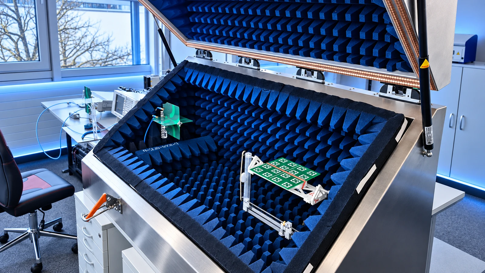
Antenna measurement in the anechoic chamber of Sevskiy GmbH

EQUIPMENT

Simulation meets measurement.

3D full wave simulation with HFSS and CST, circuit and layout work as well as network analysis up to 26.5 GHz. Measurements of S-parameters, noise figure, power and IP3 support validation.

View equipment →

YOUR REQUIREMENTS

Let's discuss your requirements.

Frequency bands, installation space, housing and target values are our starting point.

SERVICES IN DETAIL
Your development task in detail.